
GPIO stands for general-purpose input/output. GPIO pins have no specific functions, thus making them multi-functional. You can connect a device to a specific GPIO pin and control it with a software program. We can configure a pin either as input/ output. Then proceed to read from (Output pin) or write to (Input pin) that specific pin using the software. SHAKTI’s vajra, pinaka and parashu have 32 GPIO pins. In this article, the various registers and functions of GPIO are explained with examples.
Step 1: Configuring the Direction register
Firstly, the direction register of GPIO has to be set in GPIO_DIRECTION_CNTRL_REG (32-bit register). It configures the required GPIO pin(s) either as input or output.
- 0 – Input
- 1 – Output
For instance, if GPIO_DIRECTION_CNTRL_REG is set as 0000 0000 0000 0001(binary). Here, GPIO 1 is the output pin. All the others are configured as input pins.
Step 2: Reading/Writing to the GPIO Pin using DATA register
After configuring the pin as input or output, we can read from or write to the respective GPIO pin. GPIO_DATA_REG (32-Bit) is the register which holds the input data to GPIO or output data from GPIO.
For instance, Consider the following
GPIO_DIRECTION_CNTRL_REGholds 0000 0000 0000 0011(binary), i.e GPIO0 & GPIO1 are output pins; Others input.- Now,
GPIO_DATA_REGholds the value0000 0000 0000 0101(binary).- Here, GPIO0(Output) is set as 1, so that the LED/sensor connected to it receives a high signal.
- Also, GPIO2(Input) is set as 1, which means GPIO2 gets a HIGH signal from the button/switch.
Example 1: Reading from a GPIO Input pin
Let’s take an example program, where all the GPIO pins are configured as input and we read from it.
The switch/Button is connected to GPIO pins.
- GPIOn (n=0, 1, ..) to switch/button (one leg)
- Switch/Button (second leg) to VCC
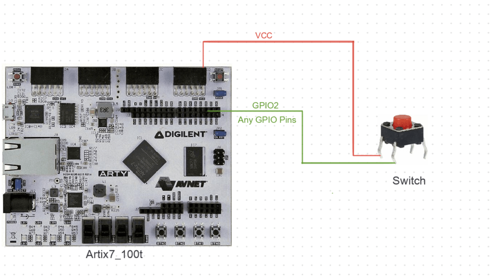
Whenever the SWITCH/button is pressed, a high signal is sent to the respective GPIO pin and that gets printed from the GPIO_DATA_REG.
#include <stdio.h>
#include "gpio.h"
#include "utils.h"
#include "platform.h"

void main()
{
unsigned long data = 0;
write_word(GPIO_DIRECTION_CNTRL_REG, 0x00000000);//Setting all pins as input
while (1) {
	data =read_word(GPIO_DATA_REG);//copy GPIO_DATA_REG content
	log_info("\n Read Data is :%x", data);
	delay_loop(3000, 5000);
	}
}
Output,
Note: Change the connection from GPIO0 to other GPIO’s during execution.
SHAKTI PROCESSORS

Booting... vspi1.0

Booting on Vajra! hart 0
Vajra is a SoC build on top of Artix7 100T.
The core belongs to Shakti C class, 64 bit.


Supported ISA: RV64IMACSU.
Processor Arch ID: f.

 Read Data is :0000
 Read Data is :0000
 Read Data is :0001 #Connected to GPIO 0; The switch is pressed
 Read Data is :0000
 Read Data is :0002 #Connected to GPIO 1; The switch is pressed
 Read Data is :0000
 Read Data is :0000
 Read Data is :0004 #Connected to GPIO 2; The switch is pressed
 Read Data is :0000
 Read Data is :0000
 Read Data is :0008 #Connected to GPIO 3; The switch is pressed
 Read Data is :0008
The pins that get the HIGH Signal from the SWITCH/BUTTON are printed as output. Consider the following table, which contains the pins receiving the high signal and the value of the data register.
Note: In arty A7 boards, for JA, JB, JC, JD, the pin configuration is as follows,
For instance, in JA, 1st pin is called JA [1].
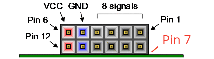
Credit: Arty A7 Reference Manual
| PIN | Pin Mapping | DATA Reg Value i.e OUTPUT (HEX) | Binary equivalent |
|---|---|---|---|
| GPIO0 | IO0 | 0001 | 0000 0000 0000 0001 |
| GPIO1 | IO1 | 0002 | 0000 0000 0000 0010 |
| GPIO2 | IO2 | 0004 | 0000 0000 0000 0100 |
| GPIO3 | IO3 | 0008 | 0000 0000 0000 1000 |
| GPIO4 | IO4 | 0010 | 0000 0000 0001 0000 |
| GPIO5 | IO5 | 0020 | 0000 0000 0010 0000 |
| GPIO6 | IO6 | 0040 | 0000 0000 0100 0000 |
| GPIO7 | IO7 | 0080 | 0000 0000 1000 0000 |
| GPIO8 | IO8 | 0100 | 0000 0001 0000 0000 |
| GPIO9 | IO9 | 0200 | 0000 0010 0000 0000 |
| GPIO10 | IO10 | 0400 | 0000 0100 0000 0000 |
| GPIO11 | IO11 | 0800 | 0000 1000 0000 0000 |
| GPIO12 | IO12 | 1000 | 0001 0000 0000 0000 |
| GPIO13 | IO13 | 2000 | 0010 0000 0000 0000 |
| GPIO14 | JB [3] | 4000 | 0100 0000 0000 0000 |
| GPIO15 | JB [4] | 8000 | 1000 0000 0000 0000 |
Note: GPIO 16 -19 are On-board LED’s and GPIO 20 -23 are On-board Push buttons
| PIN | Pin Mapping | DATA Reg Value i.e OUTPUT (HEX) | Binary equivalent |
|---|---|---|---|
| GPIO24 | JD [1] | 1000000 | 0000 0001 0000 0000 0000 0000 0000 0000 |
| GPIO25 | JD [2] | 2000000 | 0000 0010 0000 0000 0000 0000 0000 0000 |
| GPIO26 | JD [3] | 4000000 | 0000 0100 0000 0000 0000 0000 0000 0000 |
| GPIO27 | JD [4] | 8000000 | 0000 1000 0000 0000 0000 0000 0000 0000 |
| GPIO28 | JD [7] | 10000000 | 0001 0000 0000 0000 0000 0000 0000 0000 |
| GPIO29 | JD [8] | 20000000 | 0010 0000 0000 0000 0000 0000 0000 0000 |
| GPIO30 | JD [9] | 40000000 | 0100 0000 0000 0000 0000 0000 0000 0000 |
| GPIO31 | JD [10] | 80000000 | 1000 0000 0000 0000 0000 0000 0000 0000 |
Let’s see what happens when more than 1 pin receives the input signal from a button/switch.
| PIN | DATA Register Value i.e OUTPUT(HEX) | Binary equivalent |
|---|---|---|
| GPIO0, GPIO1 | 0003 | 0000 0000 0000 0011 |
| GPIO1, GPIO11 | 0802 | 0000 1000 0000 0010 |
| GPIO2, GPIO10 | 0404 | 0000 0100 0000 0100 |
| GPIO3, GPIO5 | 0028 | 0000 0000 0010 1000 |
Example 2: Writing to a number of OUTPUT GPIO pins
- In this example,
GPIO(0 to 23) pins are configured as output pins. - Firstly, Connect GPIO0 to an LED.
- Whenever the bit corresponding to the specific GPIO0 changes to 1 (HIGH)in the GPIO_DATA_REG
[0000 0000 0000 0001],the LED glows. - When the GPIO_DATA_REG changes to 0, the LED turns off.
- Whenever the bit corresponding to the specific GPIO0 changes to 1 (HIGH)in the GPIO_DATA_REG
- Now when we write
[0000 0000 1111 1111 1111 1111 1111 1111], All the LEDs connected to GPIO0 to GPIO23 will glow.
#include "platform.h"
#include "utils.h"
#include "gpio.h"

void togglegpio()
{
//Assumption 1 ---> output, 0 ---> input
	write_word(GPIO_DIRECTION_CNTRL_REG, 0x00FFFFFF); //GPIO0 to 23-> output

	while (1) {
	write_word(GPIO_DATA_REG, 0x00FFFFFF);//GPIO0 to 23 set as 1 (HIGH)
	delay_loop(1000, 5000);
	write_word(GPIO_DATA_REG, 0x00); GPIO0 to 23 set as 0 (LOW)
	delay_loop(1000, 5000);
	}
}

void main()
{
	togglegpio();
	return 0;
}
Now all the on-board LEDs and the LED connected to GPIO0 will toggle between on and off.
Example 3: Press a button to turn on a LED
In this example, we are going to use on-board Buttons (GPIO20 – GPIO23) and on-board LEDs (GPIO16 – GPIO19) also.
Steps,
- Firstly, configure
GPIO0, GPIO16, GPIO17, GPIO18, and GPIO19as OUTPUT pins inGPIO_DIRECTION_CNTRL_REG. - When on-board
Btn1is pressed, LED connected to GPIO0 glows - and when on-board
Btn2is pressed on-board LED1 and the led connected to GPIO0 glows - When on-board
Btn3is pressed, All the LEDs are turned off.
#include <stdio.h>
#include "gpio.h"
#include "utils.h"
#include "platform.h"

void main()
{
unsigned long a = 0, b = 0, c=0;
write_word(GPIO_DIRECTION_CNTRL_REG,  GPIO0| GPIO16| GPIO17| GPIO18| GPIO19); //GPIO 0,16,17,18,19 is output, other pins input
write_word(GPIO_DATA_REG, 0X0);
printf("\n----------Press Onboard Btn1 for LED1 \t BTN2= Both LED 1 and LED 2 \t BTN3=LED off------");
while (1) {
	a =read_word(GPIO_DATA_REG) & GPIO20;//reads GPIO20's high signal
	b =read_word(GPIO_DATA_REG) & GPIO21;//reads GPIO21's high signal
	c =read_word(GPIO_DATA_REG) & GPIO22;//reads GPIO22's high signal
       log_info("\n Reading Btn1 :%x", a);
	log_info("\t Reading Btn2 :%x", b);
	log_info("\t Reading Btn3 :%x", c);
	if (a) {
	write_word(GPIO_DATA_REG, GPIO0); //GPIO0's LED glows
	printf("\n LED on");
	}
	if (b) {
	write_word(GPIO_DATA_REG, GPIO16 | GPIO0); //GPIO0's LED glows and onboard LED 4
	printf("\n On-board LED on");
	}
	if (c) {
	write_word(GPIO_DATA_REG, 0x0);
	printf("\n All LEDs Off");
	}
	delay_loop(3000, 5000);
	}
}
Akshaya currently works at the RISE labs. Her favorite subjects are Web designing and Microprocessors. She loves learning about new things and writing about them!